
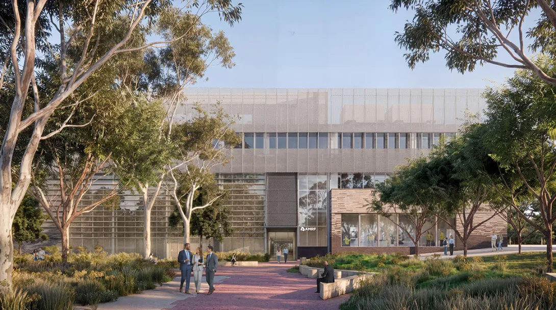
The AMRF Semiconductor Advanced Packaging Facility will serve as Australia’s first commercial advanced packaging facility, acting as a focal point for collaboration, skills development, and investment.
Construction is already underway, with the facility expected to be available from 2028.
Purpose
The facility’s capabilities are designed with flexibility at the core, facilitating three overarching goals:
- Enable Australian and international companies and research organisations to develop, validate, and scale advanced packaging solutions, with the ability to also provide low-volume production for high-value devices.
- Connect global semiconductor expertise with Australia’s growing technology ecosystem, creating new pathways into international markets, supply chains and collaborative R&D.
- Build Australia’s sovereign semiconductor capability, and strengthen strategic technology resilience, through secure supply chains and trusted partnerships.
Capability overview
The AMRF Semiconductor Advanced Packaging Facility is expected to operate a split fab model, combining back-end-of-line (BEOL) and advanced packaging technologies with the ability to test, validate, and certify semiconductor packages for long-term performance and quality. The focus will be on low volume, high value manufacturing at development and pilot scale, using commercial-grade equipment and processes.
The facility will deliver advanced packaging capabilities commencing with flip‑chip assembly techniques and progressing toward more complex integration architectures such as fan‑out wafer‑level packaging, 2.5D, and 3D packages.
The AMRF will seek an international operating partner to help finalise the facility’s capability plans and operating model. This will ensure the facility is shaped by the partner’s technical expertise and aligned with shared strategic priorities.
Operating model
The AMRF is seeking a long-term international partner to operate the purpose-built semiconductor advanced packaging facility and shape its technology roadmap.
The partner will support knowledge transfer and workforce development, creating a foundation for mutual growth in Australia and the global semiconductor ecosystem.
Facility available from 2028.
Why partner with AMRF?
- Expand manufacturing capability through ready-built cleanrooms with minimal upfront capital cost
- Shape the facility’s technical roadmap and operating model to expand your advanced packaging portfolio
- De-risk market entry with access to high value opportunities through co-location in the AMRF advanced industry ecosystem
- Accelerate R&D through collaboration opportunities with industry, research and government networks
- Minimise investment risk with a government-backed facility
- Capture new market opportunities in growing defence, quantum, sensing, medtech and advanced technology sectors
- Connect to global markets via Western Sydney 24/7 International Airport
Market process
The AMRF will run a market sounding process, followed by a Request for Proposal (RFP), to select an International operating partner ahead of the facility opening in 2028.
Interested in learning more about the partnership opportunity? Email [email protected]
The Second Building in Bradfield City
Australia’s first commercial semiconductor advanced packaging facility will be located within Bradfield City’s Second Building, which is now under development in the AMRF Precinct. The building will also house a Manufacturing Hall, designed to support activities from research and prototyping to manufacturing at scale.
Find out more about the Second Building on the Bradfield City website.